1. Material Principles and Architectural Attributes of Alumina Ceramics
1.1 Crystallographic and Compositional Basis of α-Alumina
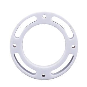
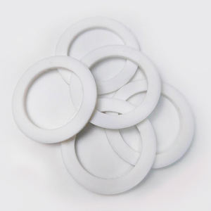
(Alumina Ceramic Substrates)
Alumina ceramic substrates, largely composed of aluminum oxide (Al two O ₃), serve as the backbone of modern-day digital packaging as a result of their exceptional balance of electric insulation, thermal security, mechanical stamina, and manufacturability.
The most thermodynamically stable phase of alumina at heats is diamond, or α-Al ₂ O TWO, which crystallizes in a hexagonal close-packed oxygen latticework with aluminum ions inhabiting two-thirds of the octahedral interstitial sites.
This thick atomic arrangement imparts high firmness (Mohs 9), superb wear resistance, and strong chemical inertness, making α-alumina appropriate for severe operating settings.
Industrial substrates typically have 90– 99.8% Al ₂ O THREE, with small additions of silica (SiO ₂), magnesia (MgO), or uncommon earth oxides utilized as sintering help to promote densification and control grain development during high-temperature processing.
Higher pureness qualities (e.g., 99.5% and over) show exceptional electrical resistivity and thermal conductivity, while lower purity variations (90– 96%) supply affordable remedies for much less demanding applications.
1.2 Microstructure and Defect Engineering for Electronic Reliability
The performance of alumina substratums in electronic systems is seriously based on microstructural uniformity and defect reduction.
A fine, equiaxed grain framework– normally ranging from 1 to 10 micrometers– guarantees mechanical stability and decreases the probability of crack breeding under thermal or mechanical stress and anxiety.
Porosity, especially interconnected or surface-connected pores, must be decreased as it breaks down both mechanical stamina and dielectric efficiency.
Advanced processing strategies such as tape casting, isostatic pushing, and regulated sintering in air or managed atmospheres enable the manufacturing of substrates with near-theoretical density (> 99.5%) and surface area roughness below 0.5 µm, essential for thin-film metallization and wire bonding.
Furthermore, impurity segregation at grain limits can result in leakage currents or electrochemical movement under prejudice, requiring rigorous control over raw material purity and sintering problems to make sure long-lasting reliability in humid or high-voltage environments.
2. Manufacturing Processes and Substrate Construction Technologies
( Alumina Ceramic Substrates)
2.1 Tape Spreading and Eco-friendly Body Processing
The manufacturing of alumina ceramic substrates begins with the preparation of an extremely dispersed slurry containing submicron Al two O three powder, organic binders, plasticizers, dispersants, and solvents.
This slurry is processed by means of tape casting– a continuous method where the suspension is topped a relocating provider movie using an accuracy medical professional blade to achieve consistent density, normally in between 0.1 mm and 1.0 mm.
After solvent dissipation, the resulting “green tape” is adaptable and can be punched, drilled, or laser-cut to form via openings for upright interconnections.
Numerous layers might be laminated flooring to produce multilayer substratums for intricate circuit assimilation, although most of industrial applications make use of single-layer arrangements due to set you back and thermal growth considerations.
The environment-friendly tapes are then thoroughly debound to remove natural ingredients with regulated thermal disintegration prior to last sintering.
2.2 Sintering and Metallization for Circuit Combination
Sintering is conducted in air at temperature levels in between 1550 ° C and 1650 ° C, where solid-state diffusion drives pore elimination and grain coarsening to attain full densification.
The linear shrinking during sintering– generally 15– 20%– need to be specifically predicted and compensated for in the layout of environment-friendly tapes to make certain dimensional accuracy of the last substratum.
Adhering to sintering, metallization is related to develop conductive traces, pads, and vias.
2 key methods control: thick-film printing and thin-film deposition.
In thick-film innovation, pastes including metal powders (e.g., tungsten, molybdenum, or silver-palladium alloys) are screen-printed onto the substratum and co-fired in a reducing environment to create durable, high-adhesion conductors.
For high-density or high-frequency applications, thin-film processes such as sputtering or dissipation are utilized to deposit bond layers (e.g., titanium or chromium) complied with by copper or gold, enabling sub-micron patterning through photolithography.
Vias are loaded with conductive pastes and terminated to establish electrical affiliations between layers in multilayer styles.
3. Practical Properties and Performance Metrics in Electronic Equipment
3.1 Thermal and Electric Actions Under Functional Stress
Alumina substratums are prized for their beneficial combination of modest thermal conductivity (20– 35 W/m · K for 96– 99.8% Al ₂ O TWO), which makes it possible for efficient warmth dissipation from power gadgets, and high volume resistivity (> 10 ¹⁴ Ω · centimeters), ensuring marginal leakage current.
Their dielectric continuous (εᵣ ≈ 9– 10 at 1 MHz) is steady over a wide temperature level and regularity range, making them suitable for high-frequency circuits approximately a number of gigahertz, although lower-κ materials like light weight aluminum nitride are chosen for mm-wave applications.
The coefficient of thermal expansion (CTE) of alumina (~ 6.8– 7.2 ppm/K) is reasonably well-matched to that of silicon (~ 3 ppm/K) and particular product packaging alloys, minimizing thermo-mechanical tension during tool procedure and thermal cycling.
Nevertheless, the CTE mismatch with silicon remains a concern in flip-chip and straight die-attach configurations, frequently needing certified interposers or underfill products to minimize exhaustion failing.
3.2 Mechanical Effectiveness and Environmental Sturdiness
Mechanically, alumina substrates exhibit high flexural toughness (300– 400 MPa) and excellent dimensional stability under lots, enabling their use in ruggedized electronic devices for aerospace, automobile, and commercial control systems.
They are immune to resonance, shock, and creep at raised temperatures, maintaining structural stability as much as 1500 ° C in inert ambiences.
In humid atmospheres, high-purity alumina shows marginal dampness absorption and exceptional resistance to ion movement, making certain lasting reliability in exterior and high-humidity applications.
Surface area firmness likewise secures versus mechanical damages throughout handling and setting up, although care should be required to prevent side breaking as a result of fundamental brittleness.
4. Industrial Applications and Technological Influence Throughout Sectors
4.1 Power Electronic Devices, RF Modules, and Automotive Systems
Alumina ceramic substrates are common in power digital modules, consisting of insulated entrance bipolar transistors (IGBTs), MOSFETs, and rectifiers, where they give electrical isolation while facilitating warmth transfer to warm sinks.
In radio frequency (RF) and microwave circuits, they serve as carrier platforms for hybrid incorporated circuits (HICs), surface area acoustic wave (SAW) filters, and antenna feed networks due to their secure dielectric properties and low loss tangent.
In the automobile market, alumina substrates are used in engine control systems (ECUs), sensor bundles, and electric automobile (EV) power converters, where they endure heats, thermal biking, and exposure to destructive fluids.
Their reliability under rough problems makes them vital for safety-critical systems such as anti-lock braking (ABS) and advanced driver help systems (ADAS).
4.2 Medical Gadgets, Aerospace, and Emerging Micro-Electro-Mechanical Solutions
Past customer and commercial electronic devices, alumina substrates are utilized in implantable medical gadgets such as pacemakers and neurostimulators, where hermetic sealing and biocompatibility are paramount.
In aerospace and protection, they are used in avionics, radar systems, and satellite communication modules because of their radiation resistance and stability in vacuum atmospheres.
In addition, alumina is significantly used as a structural and protecting platform in micro-electro-mechanical systems (MEMS), including pressure sensors, accelerometers, and microfluidic tools, where its chemical inertness and compatibility with thin-film processing are useful.
As electronic systems continue to require higher power densities, miniaturization, and reliability under severe problems, alumina ceramic substratums continue to be a cornerstone material, bridging the gap in between performance, cost, and manufacturability in sophisticated digital packaging.
5. Supplier
Alumina Technology Co., Ltd focus on the research and development, production and sales of aluminum oxide powder, aluminum oxide products, aluminum oxide crucible, etc., serving the electronics, ceramics, chemical and other industries. Since its establishment in 2005, the company has been committed to providing customers with the best products and services. If you are looking for high quality alumina rods, please feel free to contact us. (nanotrun@yahoo.com)
Tags: Alumina Ceramic Substrates, Alumina Ceramics, alumina
All articles and pictures are from the Internet. If there are any copyright issues, please contact us in time to delete.
Inquiry us